A Counter is a device which stores (and sometimes displays) the number of times a
particular event or process has occurred, often in relationship to a clock signal.
Counter Classification
-
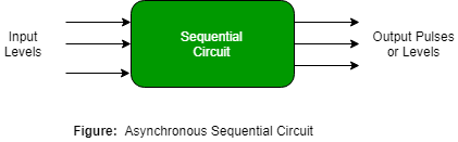
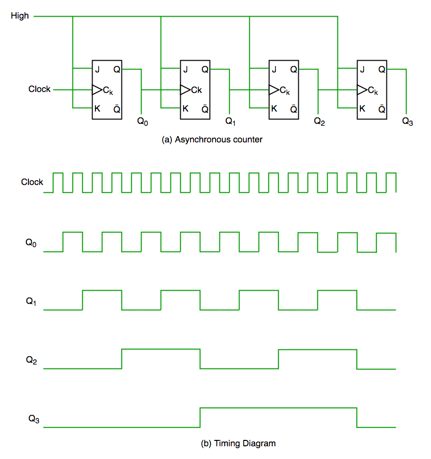
Asynchronous counter
In asynchronous counter we don’t use universal clock, only first flip flop is driven by main
clock and the clock input of rest of the following flip flop is driven by output of previous
flip flops. We can understand it by following diagram-
-
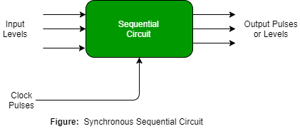
Synchronous counter
Unlike the asynchronous counter, synchronous counter has one global clock which drives each
flip flop so output changes in parallel. The one advantage of synchronous counter over
asynchronous counter is, it can operate on higher frequency than asynchronous counter as it
does not have cumulative delay because of same clock is given to each flip flop.

Design counter for given sequence -
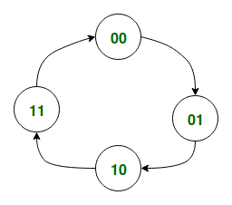
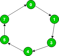
Problem Design synchronous counter for sequence: 0 → 1 → 3 → 4 → 5 → 7 → 0, using T
flip-flop.
Step-1:For given sequence, state transition diagram as following below:
Step-2:State transition table for given sequence:
| Q3 |
Q2 |
Q1 |
Q3(t+1) |
Q2(t+1) |
Q1(t+1) |
| 0 |
0 |
0 |
0 |
0 |
1 |
| 0 |
0 |
1 |
0 |
1 |
1 |
| 0 |
1 |
1 |
1 |
0 |
0 |
| 1 |
0 |
0 |
1 |
0 |
1 |
| 1 |
0 |
1 |
1 |
1 |
1 |
| 1 |
1 |
1 |
0 |
0 |
0 |
Step-3:T flip-flop – If value of Q changes either from 0 to 1 or from 1 to 0 then
input for T flip-flop is 1 else input value is 0.
| Qt |
Qt+1 |
T |
| 0
| 0 |
0 |
| 0 |
1 |
1 |
| 1 |
0 |
1 |
| 1 |
1 |
0 |
Draw input table of all T flip-flops by using the excitation table of T flip-flop. As nature of T
flip-flop is toggle in nature. Here, Q3 as Most significant bit and Q1 as least significant bit.
| Input table of Flip-Flops |
| T3 |
T2 |
T1 |
| 0 |
0 |
1 |
| 0 |
1 |
0 |
| 1
| 1 |
1 |
| 0 |
0 |
1 |
| 0 |
1 |
0 |
| 1 |
1 |
1 |
T3 = Q2, T2 = Q1, T1 =
Q'2
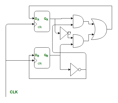
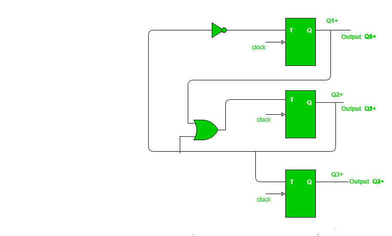
Step-4:design required circuit using expressions of K-maps:
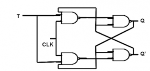
Ripple Counter
A n-bit ripple counter can count up to 2n states. It is also known as MOD n counter. It is
known as ripple counter because of the way the clock pulse ripples its way through the flip-flops.
Some of the features of ripple counter are:
- It is an asynchronous counter.
- Different flip-flops are used with a different clock pulse.
- All the flip-flops are used in toggle mode.
- Only one flip-flop is applied with an external clock pulse and another flip-flop clock is
obtained from the output of the previous flip-flop.
- The flip-flop applied with external clock pulse act as LSB (Least Significant Bit) in the
counting sequence.
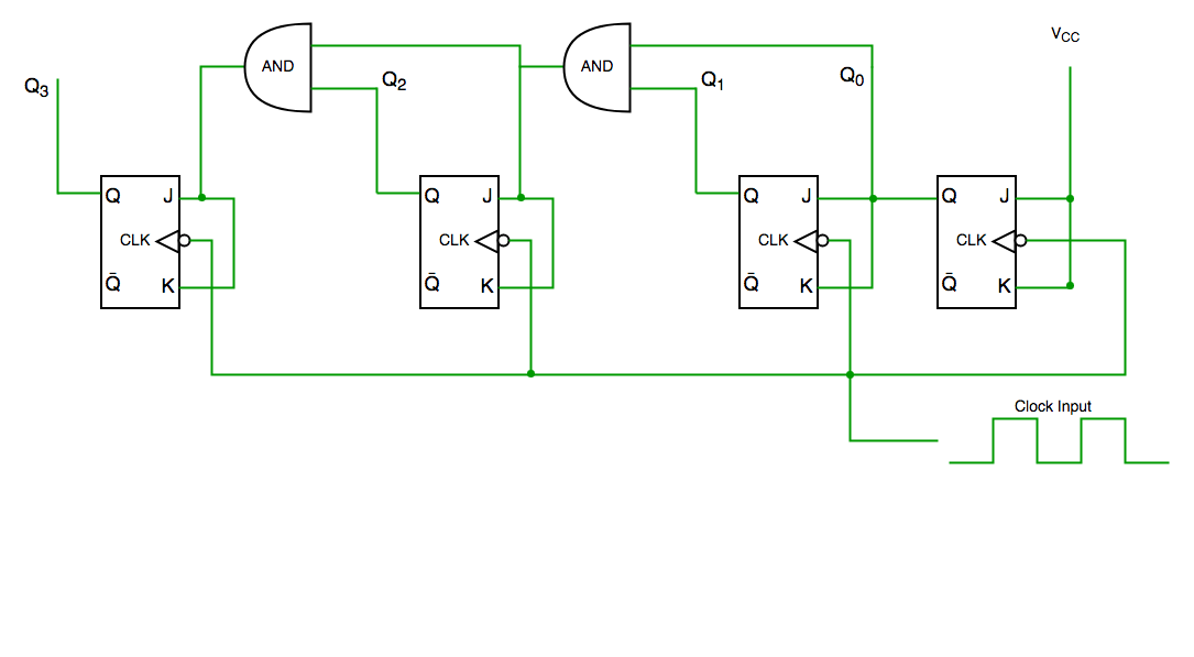
A 3-bit Ripple counter using JK flip-flop –
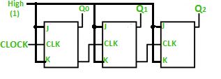
Truth Table –
| Counter State |
Q2 |
Q1 |
Q0 |
| 0 |
0 |
0 |
0 |
| 1 |
0 |
0 |
1 |
| 2 |
0 |
1 |
0 |
| 3 |
0 |
1 |
1 |
| 4 |
1 |
0 |
0 |
| 5 |
1 |
0 |
1 |
| 6 |
1 |
1 |
0 |
| 7 |
1 |
1 |
1 |
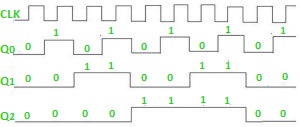
Timing diagram –
Let us assume that the clock is negative edge triggered so above counter will act as an up counter
because the clock is negative edge triggered and output is taken from Q.
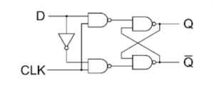
Shift Registers
The information stored within these registers can be transferred with the help of shift registers.
Shift Register is a group of flip flops used to store multiple bits of data.
Shift registers are basically of 4 types. These are:
- Serial In Serial Out shift register
- Serial In parallel Out shift register
- Parallel In Serial Out shift register
- Parallel In parallel Out shift register
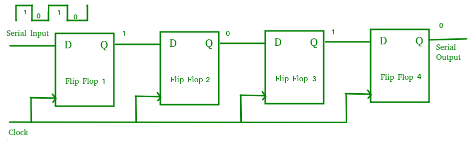
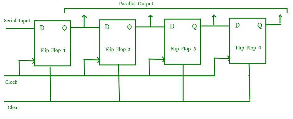
Serial-In Parallel-Out shift Register (SIPO) –
the register is loaded with serial data, one bit at a time, with the stored data being available at
the output in parallel form.
Serial-in to Serial-out (SISO) -
the data is shifted serially “IN” and “OUT” of the register, one bit at a time in either a left or
right direction under clock control.
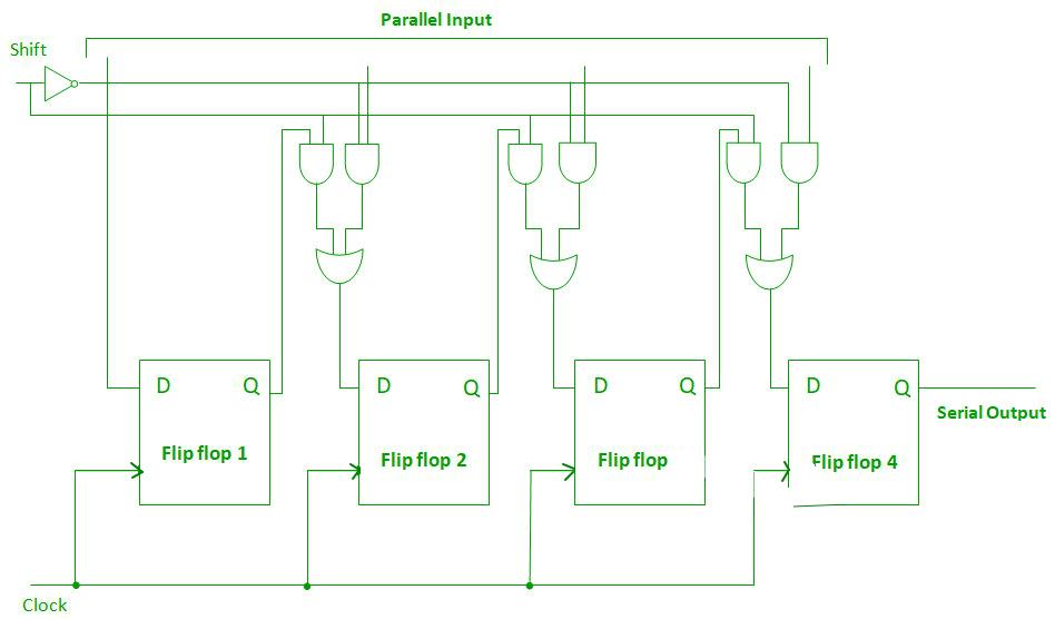
Parallel-In Serial-Out Shift Register (PISO) –
the parallel data is loaded into the register simultaneously and is shifted out of the register
serially one bit at a time under clock control.
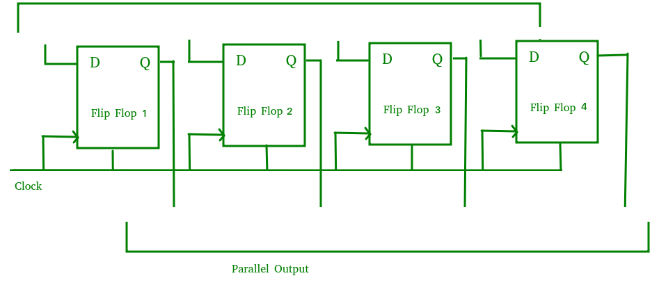
Parallel-In Parallel-Out Shift Register (PIPO) –
the parallel data is loaded simultaneously into the register, and transferred together to their
respective outputs by the same clock pulse.
Applications of shift Registers –
-
The shift registers are used for temporary data storage.
-
The shift registers are also used for data transfer and data manipulation.
-
The serial-in serial-out and parallel-in parallel-out shift registers are used to produce time
delay to digital circuits.
-
A Parallel in Serial out shift register us used to convert parallel data to serial data.