Combinational circuit design

Procedure –

  1. Identify the number of inputs and outputs of the circuit..
  2. Creating the Truth Table.
  3. Simplify the Boolean function for each output.
  4. Constructing circuit using Boolean function obtained from third step.
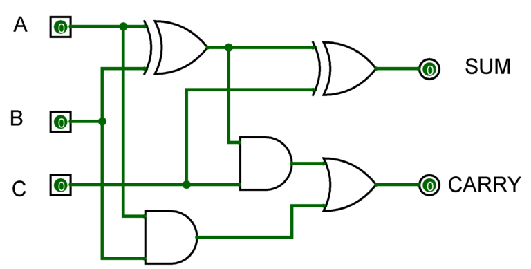
Example -

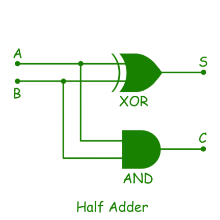
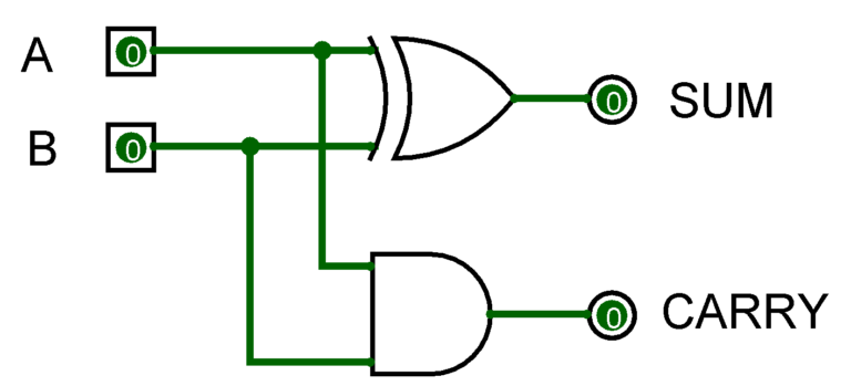
Q) we have to create a circuit that can add two bits.

Step 1: we require two inputs (A, B) and two outputs one for sum (S) of two bits and another for carry (C).

Step 2:

AB Sum Carry
00 0 1
01 1 0
10 1 0
11 0 1

Step 3:
   For Sum,
    Sum = A'B + AB' = A XOR B
   For Carry,
    Carry = AB = A AND B

Step 4:
...

Binary Adder
Half Adder

Truth table

INPUT OUTPUT
A B CARRY SUM
0 0 0 0
0 1 0 1
1 0 0 1
1 1 1 0

Simplified Boolean functions

SUM = A'B+AB' or A⊕B
CARRY = AB

Implementation

...

Implementation using NAND gates

...

Implementation using NOR gates

...
Full Adder

Truth table

INPUT OUTPUT
A B C CARRY SUM
0 0 0 0 0
0 0 1 0 1
0 1 0 0 1
0 1 1 1 0
1 0 0 0 1
1 0 1 1 0
1 1 0 1 0
1 1 1 1 1

Simplified Boolean functions

SUM = A'B'C+A'BC'+AB'C'+ABC or A⊕B⊕C
CARRY = AB+AC+BC

Implementation

...

Implementation using NAND gates

...

Implementation using NOR gates

...
Binary Subtractor
Half Subtractor

Truth table

INPUT OUTPUT
A B DIFF BORROW
0 0 0 0
0 1 1 1
1 0 1 0
1 1 0 0

Simplified Boolean functions

DIFF = A'B+AB' or A⊕B
BORROW = A'B

Implementation

...

Implementation using NAND gates

...

Implementation using NOR gates

...
Full Subtractor

Truth table

INPUT OUTPUT
A B C DIFF BORROW
0 0 0 0 0
0 0 1 1 1
0 1 0 1 1
0 1 1 0 1
1 0 0 1 0
1 0 1 0 0
1 1 0 0 0
1 1 1 1 1

Simplified Boolean functions

DIFF = A'B'C+A'BC'+AB'C'+ABC or A⊕B⊕C
BORROW = A'B+A'C+BC

Implementation

...

Implementation using NAND gates

...

Implementation using NOR gates

...
Binary Parallel adder

Parallel Adder is a digital circuit capable of finding the arithmetic sum of two binary numbers that is greater than one bit in length by operating on corresponding pairs of bits in parallel

Addition of n-bit numbers requires a chain of n full adders or a chain of one-half adder and n - 1 full adders.

...

Advantages of parallel Adder

  1. The parallel adder performs the addition operation faster as compared to serial adder.
  2. Time required for addition does not depend on the number of bits.
  3. The output is in parallel form i.e all the bits are added at the same time.

Disadvantages of parallel Adder

  1. Each adder has to wait for the carry which is to be generated from the previous adder in chain.
  2. The propagation delay( delay associated with the travelling of carry bit) is found to increase with the increase in the number of bits to be added.
Parity Generator and Checker

The parity generating technique is one of the most widely used error detection techniques for the data transmission.

The basic principle involved in the implementation of parity circuits is that sum of odd number of 1s is always 1 and sum of even number of 1s is always zero.


Parity Generator

It is combinational circuit that accepts an n-1 bit stream data and generates the additional bit that is to be transmitted with the bit stream.

In even parity bit scheme, the parity bit is ‘0’ if there are even number of 1s in the data stream and the parity bit is ‘1’ if there are odd number of 1s in the data stream.

In odd parity bit scheme, the parity bit is ‘1’ if there are even number of 1s in the data stream and the parity bit is ‘0’ if there are odd number of 1s in the data stream. Let us discuss both even and odd parity generators.

Truth table -

3-bit message Even parity bit Odd parity bit
ABC P P
000 0 1
001 1 0
010 1 0
011 0 1
100 1 0
101 0 1
110 0 1
111 1 0

(Even) P = A ⊕ B ⊕ C

...

(Odd) P = A ⊕ B Ex-NOR C

...

Parity Checker

Even Parity Checker

4-bit message Parity check
ABC P Cp
000 0 0
000 1 1
001 0 1
001 1 0
010 0 1
010 1 0
011 0 0
011 1 1
100 0 1
100 1 0
101 0 0
101 1 1
110 0 0
110 1 1
111 0 1
111 1 0

(Even) Cp = (A ⊕ B) ⊕ (C ⊕ P)

...

Odd Parity Checker

4-bit message Parity check
ABC P Cp
000 0 1
000 1 0
001 0 0
001 1 1
010 0 0
010 1 1
011 0 1
011 1 0
100 0 0
100 1 1
101 0 1
101 1 0
110 0 1
110 1 0
111 0 0
111 1 1

(Odd) Cp = (A Ex-NOR B) Ex-NOR (C Ex-NOR P)

...
Array multiplier

An array multiplier is a digital combinational circuit used for multiplying two binary numbers by employing an array of full adders and half adders.

Example -

...

product term P can be written as:-

  1. P(0)= a0b0
  2. P(1)= a1b0 + b1a0
  3. P(2) = a1b1 + c1 where c1 is the carry generated during the addition for the P(1) term.
  4. P(3) = c2 where c2 is the carry generated during the addition for the P(2) term.

combinational circuit -

...

****
 For J multiplier bit and K multiplicant bit then,
  - Number of AND gate = JxK req.
  - Number of adder = (J-1)K req.
  - Final product consist of J+K bits terms.

****

Decoders & Encoder

Decoders

A decoder is a combinational circuit that converts binary information from n input lines to a maximum of 2^n unique output lines.

2 : 4 Binary Decoder –

Truth Table:


Logical expression :

Q0 = A’B’
Q1 = A’B
Q2 = AB’
Q3 = AB

Implemented:


Encoders

An Encoder is a combinational circuit that performs the reverse operation of Decoder.It has maximum of 2^n input lines and ‘n’ output lines.

4 : 2 Encoder –

Truth table:

Logical expression for A1 & A0:

A1 = Y3 + Y2
A0 = Y3 + Y1

Implemented using OR gates :


8 : 3 Encoder (Octal to Binary) –

Truth table

Logical expression for A2, A1 & A0:

A2 = Y7 + Y6 + Y5 + Y4
A1 = Y7 + Y6 + Y3 + Y2
A0 = Y7 + Y5 + Y3 + Y1

Implemented using OR gates :

Drawbacks of Normal Encoders –

  1. There is an ambiguity, when all outputs of encoder are equal to zero.
  2. If more than one input is active High, then the encoder produces an output, which may not be the correct code.
Multiplexers

It is a combinational circuit which have many data inputs and single output depending on control or select inputs.​
Multiplexers are mainly used to increase amount of the data that can be sent over the network within certain amount of time and bandwidth.

Truth table

Implemented using OR gates :


  • a 4:1 MUX using 2:1 MUX
  • b 16:1 MUX using 4:1 MUX

Solving multiplexer circuit –

  • Firstly truth table is constructed for the given multiplexer.
  • Select lines in multiplexer are considered as input for the truth table.
  • Output in truth table can be four forms i.e. ( 0, 1, Q, Q’).
  • Now with the help of truth table we find the extended expression.
  • Then the expression is minimized using boolean algebraic rules.
  • Final function can be either in expression form or in SOP or POS form.

Example -

Given MUX,

Step 1: According to the circuit,
I1 = A
I2 = A'
I3 = 1
I4 = 0

Step 2:
f(A, B, C) = AB'C' + A'B'C + BC'.1
   = AB'C' + A'B'C + BC'(A + A')
   = AB'C' + A'B'C + ABC' + A'BC'
   = 100 001 110 010
   = m(1, 2, 4, 6)